Hot Chips When you charge hundreds of thousands of dollars per core for an engine that is designed to run full-out all day doing online transaction processing and all night running single-threaded big batch jobs, you have no choice but to believe in higher clock speeds and doing anything and everything to boost that single-thread performance. And that is what IBM's new z12 mainframe engines are all about.
Big Blue announced the System zEnterprise EC12 mainframes smack dab in the middle of the Hot Chips chippery extravaganza in Cupertino, California last week, and did so several weeks in advance of the planned launch for the systems.
IBM had planned to speak about the z12 processors at Hot Chips, and Kevin Shum, senior technical staff member for System z processor development in IBM's Systems and Technology Group. Shum told El Reg that the paper he submitted for his presentation didn't even have a die shot or talk about many of the aspects of the zEC12 system because these were not ready for primetime when he submitted his materials months ago. We already told you a little about the z12 processors and a lot about the zEC12 systems, but we can now tell you a little bit more about the z12 processors and how they are different from prior generations of mainframe engines.
The first thing to consider is that unlike other processor architectures, considering the batch orientation of mainframe jobs, where you want to start a sequential piece of work and finish as soon as possible. IBM has used its ongoing chip fabrication process improvements to ramp up the clock speeds of its processors rather than plunk a lot of cores onto a single die. IBM has used its expertise in packaging, ceramics, and cooling to cram as many hot processing elements (these z12 chips reportedly run at about 300 watts) into a rack as possible. In this case, a full-on System zEnterprise EC12-HA1 system has four processor books with five sockets sporting six-core z12 engines in each socket, for a total of 120 raw compute engines. These engines are used for a variety of tasks inside the box, and up to 101 of them can be configured to run z/OS, z/VM, z/VSE, z/TPF, or Linux, act as zIIP or zAAP coprocessors to speed up DB2 or Java workloads, or support system I/O and clustering operations.
The top-end EC12 has z12 engines that are 25 per cent more powerful, at around 1,600 MIPS, than the z11 engines used in the zEnterprise 196 servers announced two years ago. The full-on system capacity is about 50 per cent greater, at around 75,000 MIPS.
Getting that 50 per cent boost in scalability is relatively easy. Getting that 25 per cent boost in single-thread performance is very, very hard, especially when you consider that the prior-generation of mainframe engines were already running at a very high 5.2GHz.
The jump in processor speed for IBM's mainframes has been quite dramatic in the past several years:
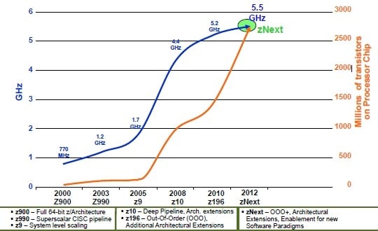
IBM has cranked the clocks on System z processors, and it has to
IBM was able to crank the clocks above 1GHz with the z6 engines in the System z990 servers back in 2003 by moving to a superscalar CISC pipeline. With the z10 engines in 2008, concurrent with a shrink to 64 nanometer processes IBM also added a much deeper pipeline, allowing the clocks to jump up to 4.4GHz and substantially improving single-threaded performance for the mainframe engines. Two years ago, IBM shifted to out-of-order execution on the z11 engine pipelines and did a shrink to 45 nanometers, pushing the clocks up to 5.2GHz. And according to Shum, a second-generation out-of-order execution stream plus the shrink to 32 nanometer processes is what is allowing IBM to get two more cores on the die while boosting the clock speed to 5.5GHz.
"The frequency runs all out, 24 by 7, because our customers run these machines all the time," bragged Shum. "And as a transactional engine, we are not just moving data from place to place, either."
The changes that IBM has made in the out-of-order execution scheme give the processor more out of order groups, allowing the pipeline to dispatch more grouped instructions and issue more micro-operations in a cycle than the prior z11 chip's pipeline. IBM has added an instruction queue to the decode/dispatch unit on the chip, and added a virtual branch unit for relative branch execution and a virtual branch queue for relative branch queuing. The instruction issue bandwidth was pumped up by 40 per cent to seven micro-ops per cycle. The improved branch prediction unit has two levels now, and has three times the capacity as the BRU in the z11 chip.
"When your pipeline is deep, branch prediction is extremely important. A lot of people brag about their branch prediction, but we have the Cadillac," boasted Shum.
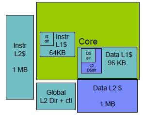
Block diagram of the z12 core
Each z12 core has 64KB of L1 instruction cache and 96KB of L1 data cache. IBM did a few funky things with the cache inside the z12 engine to keep those 5.5GHz threads fed. First, it broke the L2 cache into instruction and data caches, mirroring what most chip etchers do with L1 caches. Most of the L2 caches out there in the world are unified, meaning they are used for both data and instructions.
IBM has 1MB of L1 data cache and 1MB of L2 instruction cache on each z12 core. Big Blue also embedded the L2 data directory inside of the L1 data cache, right next to its own directory, and logically indexed the L2 data cache just like the L1 cache. What this means is that when there is an miss in the L1 data cache, the core knows it and can look it up and see if it is in L2 data cache right then and there, reducing the L2 hit latency by 45 per cent. The core includes a global L2 cache controller and directory as well to keep things in lockstep.
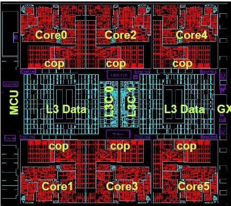
Die schematic of the z12 mainframe chip
Add it up, and the z12 core can issue seven instructions per clock, decode three instructions per clock, and complete three instructions per clock. The memory controllers on the die also support transactional memory, which we discussed elsewhere in the zEC12 system announcement last week.
The z12 processor is implemented in a 15-layer high-K metal gate process whipped up with IBM's copper/silicon-on-insulator technologies; it etches circuits at 32 nanometers in this generation. The z12 chip has 2.75 billion transistors, and includes an on-chip DDR3 memory controller (which also implements IBM's Redundant Array of Independent Memory (RAIM) parity and striping protection across memory chips. The zEC12 system supports 3TB of addressable memory, just like the z196.
The various coprocessors on the mainframe engine are now allocated to each core for them to use by their lonesome instead of being shared by the cores. (That's the "cop" in the die schematic above.) These include vector math units and encryption engines, among other things. The z12 chip has 48MB of embedded DRAM (eDRAM) L3 cache memory to feed the cores, which is twice the L3 cache the z11 processor had. There are two L3 cache controllers at the heart of the chip, as was the case with the previous z11 chips.
The off-chip SMP hub/shared L4 cache controller chip is still part of the architecture of the System z mainframe, but Shum did not talk about it during his presentation. With the zEnterprise 196 system, four z11 engines and two of these SMP hub chips, with a total of 192MB across two L4 controllers, were linked together to create a multi-chip module (MCM) that is welded onto each processor book.
We know the zEnterprise EC12 has five processor sockets in the book and that L4 cache memory has been doubled to a total of 384MB, but it is not clear if IBM just doubled up the L4 cache per SMP hub chip or doubled up the number of units on the book. The former seems likely, but the latter is possible. ®


