Posted on 09/10/2012 1:59:41 PM PDT by Ernest_at_the_Beach
Intel Labs is a super interesting arm of the company, responsible for developing technologies that would potentially go into products 5 - 10 years down the road. It's from the labs that we got things like BBUL packaging (still not deployed but neat nonetheless) and the first 10GHz x86 ALUs.
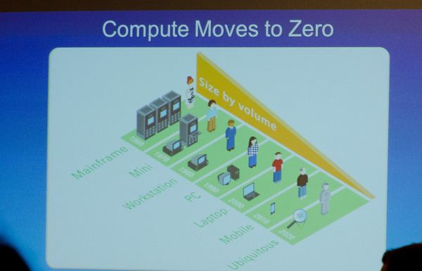
Today, on the day before IDF, Intel put together a collection of demos to give us insight into what the labs folks are working on. We're still an hour away from actual demos but Intel did share a super interesting slide, pictured above.
Moore's Law and the (almost) ever shrinking transistor give us one of two things: more complexity/performance/features in a given die area, or the same performance in a steadily decreasing die area.
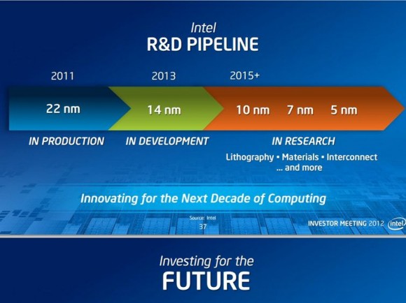
Exploiting the latter benefit, we have the realization above. By 2020, which assuming a 2 year cadence between process nodes means we're talking about silicon built on a 5nm process, Intel expects that the size of "meaningful compute" approaches zero. It's not totally clear what Intel defines as meaningful compute, but if you keep in mind that a single AMD Jaguar core measures < 3mm^2 at 28nm, it's not a stretch to believe that we'd have quite a bit of compute available nearly for free at 5nm. Assuming perfect scaling (not going to happen), a 100mm^2 die at 22nm would measure only 6.25mm^2 at 5nm. Even if you don't get prefect scaling, Moore's Law can give us the performance we get in a smartphone today in a size that's small enough and cheap enough to make that we can integrate it anywhere (smart-tables anyone?).
The idea of ubiquitous compute has been around for quite a while, but it's still mindblowing to think about what can happen once meaningful compute is really almost free. Remember that there's a direct relationship between the size of silicon and its cost. Today's 80 - 120mm^2 smartphone SoCs cost anywhere from $10 - $30 to integrate into a phone. If silicon with that level of complexity can be reduced in size to the point where we're looking at low single digit costs, the potential impact to new markets will be huge.
We saw what affordable compute did for smartphones, the next question is what even more affordable compute can do for other, undiscovered markets. A while ago I heard someone smart tell me that at some point displays become cheap enough where many surfaces we take for granted, start integrating them (e.g. bathroom mirrors that double as displays). Combine that with cheap compute that we can integrate everywhere as well and we have a recipe for the future.
Ernest, I understood just enough to say, wow, cool!
Things are gonna get interesting.
ubiquitous computing will come after they install ad screens in cereal boxes, not before...
We need someone to put up a good pictorial tutorial.
I would but everything I know is proprietary. And I don’t work for Intel.
http://en.wikipedia.org/wiki/Semiconductor_device_fabrication
Does this mean I should not sell my Intel stock?
To put this into perspective, the diameter of a single silicon atom is 0.22 nm. We will VERY soon be running into physical constraints of how small we can have a 2-dimensional circuit, and will need to go more 3-dimensional (which has its own issues regarding heat dissipation).

That etching is based on lithography, no different than what artists use. However, in order to reduce the size of the elements, they can't use visible light: The wavelength is too long. If I remember correctly, they're using X-Rays for the lithography these days. It will be difficult to take that technology very much further, unless they figure out a safe way to move to gamma rays. They're going to eventually move to "quantum computing" and light based circuitry and storage, which is already being actively researched.
Mark
Disclaimer: Opinions posted on Free Republic are those of the individual posters and do not necessarily represent the opinion of Free Republic or its management. All materials posted herein are protected by copyright law and the exemption for fair use of copyrighted works.