Skip to comments.
AMD to launch Richland on March 12 ( Follow on to the Trinity APU chip...F2 socket)
Fudzilla ^
| Tuesday, 05 March 2013 15:26
| Slobodan Simic
Posted on 03/05/2013 12:18:43 PM PST by Ernest_at_the_Beach

AMD is ready for it
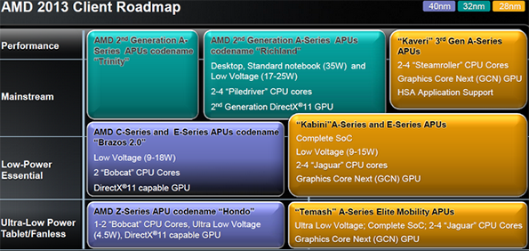
There have been more than enough leaks dealing with Richland, AMD's successor to the Trinity powered Virgo platform, and we even had a chance to see some leaks regarding its succesor, codenamed Kaveri. As you may already know, Richland is planned to last through 2013 and it is clear that this is very important chip for AMD.
Based on the Piledriver architecture and built using 32nm technology, Richland will feature an integrated GPU that will be upgraded to Radeon HD 8000 series, a generation ahead of Trinity. As you know, there has been a lot of leaks regarding the Richland parts and the quad-core A10-6800K with Radeon HD 8670D graphics is expected to pack quite a punch. Best of all, Richland will still use the same FM2 socket.
According to our sources, the NDA will be lifted on 12th of March, 8am EST, and we are sure that we will see at least a couple of reviews as well as some additional info regarding the price and the availability date.
You can check out earlier Richland leaks and rumors here.
Last modified on Tuesday, 05 March 2013 18:02
TOPICS: Business/Economy; Computers/Internet
KEYWORDS: amd; hitech; richland; trinity
To: ShadowAce
2
posted on
03/05/2013 12:20:45 PM PST
by
Ernest_at_the_Beach
((The Global Warming Hoax was a Criminal Act....where is Al Gore?))
To: Ernest_at_the_Beach
Is this the Playstation chip for the PS4?
3
posted on
03/05/2013 12:25:14 PM PST
by
GraceG
To: Ernest_at_the_Beach
I think AMD is about to pop with the new PS4 chip.
4
posted on
03/05/2013 12:29:48 PM PST
by
mnehring
To: Ernest_at_the_Beach
Awesome...an APU with a GCN GPU; exciting!
5
posted on
03/05/2013 1:29:21 PM PST
by
krb
(Obama is a miserable failure.)
To: Ernest_at_the_Beach
6
posted on
03/05/2013 1:31:56 PM PST
by
The Cajun
(Sarah Palin, Mark Levin......Nuff said.)
To: Ernest_at_the_Beach
Which of these developments is gonna get the stock price back up?
7
posted on
03/06/2013 1:40:35 AM PST
by
Mr. Blond
To: krb
I think the GNC is to be in the Kaveri ....arrives late 2013 of early 2014...
but there is some confusing technical reports.
8
posted on
03/11/2013 3:01:20 PM PDT
by
Ernest_at_the_Beach
((The Global Warming Hoax was a Criminal Act....where is Al Gore?))
To: GraceG
NO,....PS4 will use a modified Jaguar chip ...follow on to the Brazos.
9
posted on
03/11/2013 3:02:32 PM PDT
by
Ernest_at_the_Beach
((The Global Warming Hoax was a Criminal Act....where is Al Gore?))
To: The Cajun
Missed this report ,... .
AMD Richland APU Clock Speeds Revealed – Flagship A10-6800K Boosts Upto 4.4 GHz
Posted 1 month ago by Hassan Mujtaba
Over the last week, we reported the first detailed specifications of AMD’s upcoming Richland APU lineup. Planned to arrive in Q2 2013 while already shipping to OEMs, the Richland APU lineup would consist a total of six A-Series APUs including the flagship A10-6800K.
AMD Richland APU – All Set to Break 4 GHz Clock Barrier
Chinese portal of VR-Zone further details the specifications of the upcoming Richland APUs and has revealed the clock frequencies of these models. The clock speeds are quite a surprise as AMD has planned to boost its flagship APU past the 4 GHz barrier. You heard that right, the AMD A10-6800K Richland APU has a base clock of 4.1 GHz and boosts upto 4.4 GHz with AMD’s TurboCore 2.0 technology. Not only the flagship model but the other APU’s too seem to shatter the 4 GHz barrier with Turbo Boost. In addition to clock frequencies, VR-Zone specifications also list the iGPU frequencies as listed below:
- A10-6800K Radeon HD 8670D 844 MHz/ Quad Core 100W, 4.1 GHz/4.4 GHz
- A8-6600K Radeon HD 8570D 844 MHz/ Quad Core 100W, 3.9 GHz/4.2 GHz
- A10-6700 Radeon HD 8670D 844 MHz/ Quad Core 65W, 3.7 GHz/4.3 GHz
- A8-6500 Radeon HD 8570D 800 MHz/ Quad Core 65W, 3.5 GHz/4.1 GHz
- A6-6400K Radeon HD 8470D 800 MHz/ Dual Core 65W, 3.9 GHz/4.1 GHz
- A4-6300 Radeon HD 8370D 760 MHz/ Dual Core 65W, 3.7 GHz/3.9 GHz

The AMD Richland APU would be based on an enhanced version of the x86 Piledriver architecture which is built on a 32nm fabrication process. AMD Richland APU lineup would be compatible with FM2 socket motherboards fused with the A88X and A85X chipsets. The APUs allow compatibility with DDR3 DIMMs rated at 1866 MHz + O.C, while the chipset is set to support up to eight SATA 6GB/s devices with an additional 4 USB 3.0 ports and 14 USB 2.0 ports.It should be noted though that the HD 8000* IGP models on the Richland APU are based on the Southern Island GCN architecture which allow Dual GPU support with Radeon HD 7000 discrete graphic solutions. However, VR-Zone reveals that AMD would further expand their compatibility with Radeon HD 8000 discrete graphic solutions in the future when the products launch.
If you still aren’t satisfied with the specifications of Richland APU, then know this that AMD has another APU platform under its sleeves that is scheduled for a 2013 launch and its equipped with the latest 28nm steamroller cores. Yup! Kaveri Accelerated processing units are arriving by the end of this year featuring the latest GCN 2.0 Radeon HD 8000 series IGP and HSA enhancements, more here.
10
posted on
03/11/2013 3:08:49 PM PDT
by
Ernest_at_the_Beach
((The Global Warming Hoax was a Criminal Act....where is Al Gore?))
To: All
Just tacking this on here:
Analysis: AMD Kaveri APU and Steamroller Core Architectural Enhancements Unveiled
3/6/2013 by: Marcus Pollice
******************************EXCERPTS******************************************
Recently, we exclusively unveiled that Kaveri, successor to the current "Trinity" high-end APU (Fusion A8 and A10 family) features a GDDR5 memory interface. This time we will talk about architectural enhancements of AMDs upcoming mainstream APU Kaveri as well as enhancements of the Steamroller cores which will also make their way into servers and high-end desktop systems in 2014. The information comes from a "Preliminary BIOS and Kernel Developer's Guide for AMD Family 15h Models 30h-3Fh Processors" (you can find a similar document here, dated January 2012) document, available to interested developers.
11
posted on
03/11/2013 3:17:09 PM PDT
by
Ernest_at_the_Beach
((The Global Warming Hoax was a Criminal Act....where is Al Gore?))
To: All
And this:
AMD Kaveri Unveiled: PC Architecture Gets GDDR5
3/5/2013 by: Marcus Pollice
*************************************EXCERPT*************************************
We were able to take a peek at AMD NDA information (aimed at engineers) that details the technical features of the Kaveri APU. According to this information, Kaveri features a GDDR5 memory interface consisting of four 32-bit memory channels. This is perfectly matching the width of a GDDR5 chip which is also 32-bit. However, the memory controller has to be set up in a way so that two 32-bit channels work in tandem, half-channel use is not supported. The total width is 128-bit, so the main advantage comes from higher clock speeds of GDDR5 memory. This is in addition to the 128-bit DDR3 interface that we already know from previous APUs. Usage of DDR3 and GDDR5 is mutually exclusive.
While the information we glanced at is clearly preliminary and could be changed till the release of the chip, the focus should be less expensive GDDR5 chips with moderate clock speeds – not the 6GHz hotness you find in high-end graphics cards like
GeForce GTX Titan. Specifically the document lists 800 MHz QDR and 850MHz QDR (3200MHz and 3400MHz) clocks which would result with 51.2 GB/s and 54.4 GB/s of system memory bandwidth. Compared to current 25.6 GB/s with the DDR3-1600, this is quite the performance bump. The surprises don’t end there - Kaveri will support DDR3 up to 1250 MHz DDR (2500MHz) – it specifically adds 2400MHz and 2500MHz modes over
Trinity, which officially supported up to 2133MHz. Nevertheless GDDR5 would provide a tangible bandwidth improvement and might be the smarter choice given that DDR3 above 1866MHz starts to get prohibitively expensive.
We can anticipate one potential downside with GDDR5, however. Currently most commonly deployed chips only feature 2 GBit capacity, which translates to 256MB per chip. To fully populate the GDDR5 interface, you need four chips, totaling mere 1GB, which can be considered a bit low for system memory. With two chips per channel we get 2GB, which is still low but starts to get workable. We don't have any hard info on how many chips per channel are possible with GDDR5, on GPUs currently no more than two are used. Either AMD plans to have a crazy amount of GDDR5 BGA soldered to the boards, or they bet on 4 GBit chips which would bring 4GB configurations within reach or the whole GDDR5 support is meant for embedded systems with lower memory requirements. Remember that even Nvidia had to give up on the idea of selling the Tesla K20 card with 12GB memory and had to settle for 6GB. Last year, we talked with representatives from
Samsung Memory which refuted the idea of offering higher capacity GDDR5 chips but as the time goes, opinions might change.
The GDDR5 interface inside Kaveri represents a very interesting option. After
Sony made their PS4 announcement (8GB GDDR5), this step actually appeares to be a logical evolution of the APU products. Current APUs feature quite capable GPUs who are hamstrung by low memory bandwidth compared to the entry-level discrete GPUs. Even though GDDR5 memory reduces system flexibility (BGA package has to be soldered to the mainboard), the performance gain may more than make up for that.
Other changes in Kaveri include a PCIe 3.0 interface, which brings the APU in line with Intel's Ivy Bridge and Haswell CPUs. In addition to the 16 lane PCIe 3.0 interface, Kaveri features eight PCIe 2.0 lanes for general purpose use. The PCIe 3.0 interface can be configured as two x8 interfaces, thus enabling Crossfire or Discrete GPU plus Storage Card (Solid State Cards are gaining in popularity). Four of the PCIe 2.0 lanes are used to connect the Southbridge or Fusion Controller Hub (FCH) as AMD calls it, the other four lanes can be used as four x1, two x2 or one x4 connection.
We also tried to clarify if Kabini contains a GDDR5 interface as well, which is scheduled to debut around the Computex timeframe. Given that an PS4 uses significantly modified version of Kabini and utilizes GDDR5 memory, such possibility would not be unreasonable. However, from the documents we were able to look at didn't contain any information on such a feature. While this is not a 100% confirmation, Kabini with GDDR5 for the PC market probably won't happen.
Once the DDR4 memory comes along the advantages of GDDR5 start to diminish again. DDR4 will enable higher densities at comparable speeds as well as upgradeable modules which might be more desirable for customers. More importantly, we view Kaveri GDDR5 as a trial run, first generation part. As we all know,
GDDR5 will be replaced with GDDR6 in 2014 timeframe, foreshadow of what might await us down the road: APUs in BGA package soldered to the board with memory soldered to the board and next to no upgradeability. While this is not desirable from an enthusiast point of view, this is what the mass market will inevitably move to in the next few years.
12
posted on
03/11/2013 3:20:47 PM PDT
by
Ernest_at_the_Beach
((The Global Warming Hoax was a Criminal Act....where is Al Gore?))
To: Ernest_at_the_Beach
It really is confusing. Here’s my take. I think Richland does have GCN, but it still has two distinct memory regions: DDR3 for the CPU and GDDR5 for the GPU. With that setup you still need to explicitly copy buffers back and forth to make it work.
I think that Kaveri is also GCN, but with a unified memory block: both the CPUs and GPU system use the same GDDR5 memory and there is no need to copy buffers from one to the other for it to work.
If I am right, that means that a) As a developer, Richland is a great part to use for now to start writing code, and b) by the time Kaveri comes out all of the memory latency issues associated with having to copy buffers around will go away on their own.
Man I hope I’m right.
13
posted on
03/11/2013 3:57:26 PM PDT
by
krb
(Obama is a miserable failure.)
To: krb
From the link at post #10:

Note that Richland is not on it.
14
posted on
03/11/2013 4:47:02 PM PDT
by
Ernest_at_the_Beach
((The Global Warming Hoax was a Criminal Act....where is Al Gore?))
To: Ernest_at_the_Beach
In post #10:
> ports.It should be noted though that the HD 8000* IGP models on the Richland APU are based on the Southern Island GCN architecture
15
posted on
03/11/2013 4:53:52 PM PDT
by
krb
(Obama is a miserable failure.)
To: krb
I thought Sea Islands was the GCN...
16
posted on
03/11/2013 6:29:15 PM PDT
by
Ernest_at_the_Beach
((The Global Warming Hoax was a Criminal Act....where is Al Gore?))
To: krb
17
posted on
03/11/2013 6:48:29 PM PDT
by
Ernest_at_the_Beach
((The Global Warming Hoax was a Criminal Act....where is Al Gore?))
To: krb
18
posted on
03/11/2013 8:13:57 PM PDT
by
Ernest_at_the_Beach
((The Global Warming Hoax was a Criminal Act....where is Al Gore?))
To: All
At Slashdot I found this:
AMD Next-Gen Graphics May Slip To End of 2013
*************************************EXCERPT*************************
MojoKid writes
"AMD has yet to make an official statement on this topic, but several unofficial remarks and leaks point in the same direction. Contrary to rumor, there won't be a new GCN 2.0 GPU out this spring to head up the Radeon HD 8000 family. This breaks with a pattern AMD has followed for nearly six years. AMD recently refreshed its mobile product lines with HD 8000M hardware, replacing some old 40nm parts with new 28nm GPUs based on GCN (Graphics Core Next). In desktop, it's a different story. AMD is already shipping 'Radeon HD 8000' cards to OEMs, but these cards are based on HD 7000 cores with new model numbers. RAM, TDP, core counts, and architectural features are all identical to the HD 7000 lineup. GPU rebadges are nothing new, but this is the first time in at least six years that AMD has rebadged the top end of a product line. Obviously any delay in a cutthroat market against Nvidia is a non-optimal situation, but consider the problem from AMD's point of view. We know AMD built the GPU inside Wii U. It's also widely rumored to have designed the CPU and GPU for the Xbox Durango and possibly both of those components for the PS4 as well. It's possible, if not likely, that the company has opted to focus on the technologies most vital to its survival over the next 12 months." Maybe the Free GNU/Linux
drivers will be ready at launch after all.
19
posted on
03/11/2013 8:28:55 PM PDT
by
Ernest_at_the_Beach
((The Global Warming Hoax was a Criminal Act....where is Al Gore?))
Disclaimer:
Opinions posted on Free Republic are those of the individual
posters and do not necessarily represent the opinion of Free Republic or its
management. All materials posted herein are protected by copyright law and the
exemption for fair use of copyrighted works.
FreeRepublic.com is powered by software copyright 2000-2008 John Robinson

 *********************************