Free Republic
Browse · Search
News/Activism
Topics · Post Article

Skip to comments.

STMicroelectronics, GlobalFoundries to Build 300-mm Fab in Crolles
EE Times ^

Posted on 07/14/2022 11:10:15 AM PDT by FarCenter

STMicroelectronics and GlobalFoundries announced they have signed a memorandum of understanding to build a 300-mm semiconductor manufacturing facility that will help develop the fully depleted silicon-on-insulator (FD-SOI) technology ecosystem. The new facility will represent a multi-billion–euro investment and is expected to create about 1,000 jobs.

The jointly operated fab will support GlobalFoundries’ 22FDX FD-SOI process technology and STMicroelectronics’ technology roadmap down to 18 nm for automotive, industrial, IoT, and communications infrastructure applications, companies said.

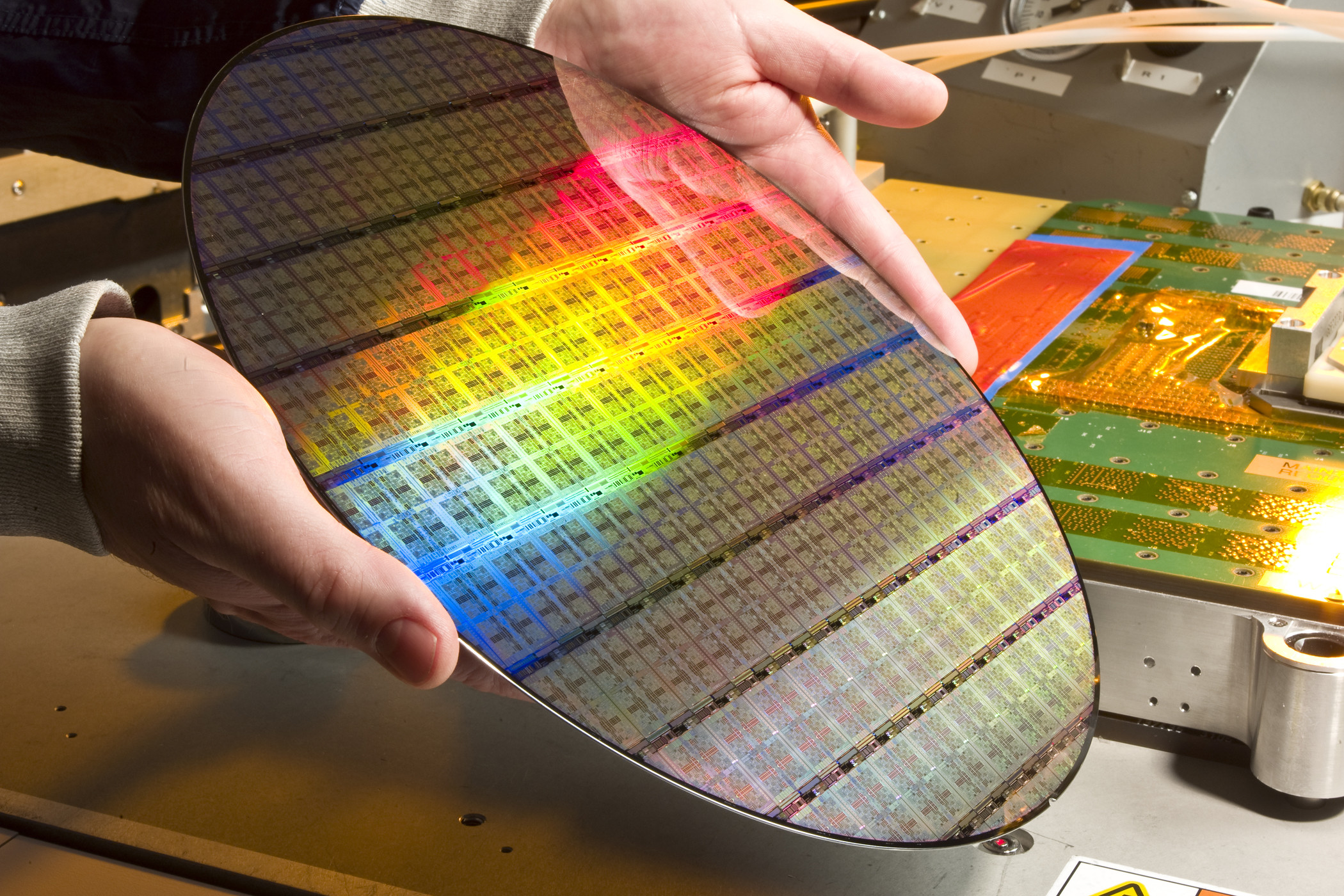
The facility, which will be adjacent to STMicroelectronics’ existing 300-mm manufacturing site in Crolles, France, is set to reach full capacity by 2026, with up to 620,000 300-mm chips per year. The breakdown will be as follows: about 42% for STMicroelectronics and about 58% for GlobalFoundries.

“This new manufacturing facility will support our $20 billion+ revenue ambition,” said Jean-Marc Chéry, president and CEO of STMicroelectronics, at a press conference held today (July 11). Moving to the strengths of the collaboration, Chéry said, “We have a long legacy partnership with GlobalFoundries. We strongly promote the FD-SOI ecosystem, and by doing it together, we will reach a bigger scale [and] go faster than everybody in Europe.”

Thomas Caulfield, CEO of GlobalFoundries, confirmed, “We have a common belief in the FD-SOI platform. ...”

Refusing to divulge the exact amount, partners indicated that the project will represent a multi-billion–euro investment and will receive “significant” financial support from the State of France. The French media sites Le Monde and Le Figaro, however, speak of an estimated investment of €5.7 billion.

The project remains subject to the execution of definitive agreements and various regulatory approvals, including from the European Commission’s Directorate-General for Competition, and to the completion of the consultation with STMicroelectronics’ French Works Council.

(Excerpt) Read more at eetimes.eu ...


TOPICS: News/Current Events
KEYWORDS: apple; crolles; europeancommission; europeanunion; france; globalfoundries; jeanmarcchery; korea; republicofkorea; semiconductors; stmicroelectronics; taiwan; thomascaulfield; tsmc
Navigation: use the links below to view more comments.
first 1-2021-24 next last

1 posted on 07/14/2022 11:10:15 AM PDT by FarCenter
[ Post Reply | Private Reply | View Replies]

To: FarCenter

That’s some big chips.😳


2 posted on 07/14/2022 11:16:18 AM PDT by BiteYourSelf ( Earth first we'll strip mine the other planets later.)
[ Post Reply | Private Reply | To 1 | View Replies]

To: FarCenter

300mm (30 cm or 11 inch transistors / microprocessors) are, well, pretty much late 1940s / early 1950s technology, no?


3 posted on 07/14/2022 11:20:41 AM PDT by lefty-lie-spy (Stay Metal)
[ Post Reply | Private Reply | To 1 | View Replies]

To: BiteYourSelf
That’s some big chips.😳

300-mm - is that 300 square mm in area, as in a 17mmx17mm die?

4 posted on 07/14/2022 11:21:06 AM PDT by Yo-Yo (Is the /Sarc tag really necessary? Pray for President Biden: Psalm 109:8)
[ Post Reply | Private Reply | To 2 | View Replies]

To: BiteYourSelf

Started at 1 1/4 inch, ended at 200 mm (IBM w/notch)


5 posted on 07/14/2022 11:21:30 AM PDT by sasquatch
[ Post Reply | Private Reply | To 2 | View Replies]

To: FarCenter

I remember back in the 1990s when the technology media was saying that we would never be able to make a chip with smaller than 25 nanometer traces due to physics limits.


6 posted on 07/14/2022 11:24:00 AM PDT by lefty-lie-spy (Stay Metal)
[ Post Reply | Private Reply | To 1 | View Replies]

To: BiteYourSelf

Jinx. I’m your friend, bro.


7 posted on 07/14/2022 11:24:56 AM PDT by lefty-lie-spy (Stay Metal)
[ Post Reply | Private Reply | To 2 | View Replies]

To: FarCenter

GF-STM have abandoned any process smaller than 14nm.
There is still plenty of demand for older technology.
Both IBM and AMD abandoned GF on 7nm as they couldn’t get it to work.


8 posted on 07/14/2022 11:25:13 AM PDT by Zathras
[ Post Reply | Private Reply | To 1 | View Replies]

To: BiteYourSelf

300 mm is the diameter of the silicon wafer. After lithography and other processing steps, the wafer is cut into the individual chips. The chips are then tested and bonded into packaging suitable for mounting on circuit boards. These latter steps are usually done in Southeast Asia, even for wafers from fabs in the US and Europe.


9 posted on 07/14/2022 11:25:34 AM PDT by FarCenter
[ Post Reply | Private Reply | To 2 | View Replies]

To: lefty-lie-spy

300mm refers to the size of the silicon wafer on which the chips will be created. A 300mm wafer will yield 640 ‘dies’ or individual chips per wafer.

https://en.wikipedia.org/wiki/Wafer_(electronics)


10 posted on 07/14/2022 11:28:13 AM PDT by Spktyr (Overwhelmingly superior firepower and the willingness to use it is the only proven peace solution.)
[ Post Reply | Private Reply | To 3 | View Replies]

To: sasquatch

200mm was passed by 300mm in 2002, which was two decades ago. 450mm is the newest proposed standard size.


11 posted on 07/14/2022 11:30:04 AM PDT by Spktyr (Overwhelmingly superior firepower and the willingness to use it is the only proven peace solution.)
[ Post Reply | Private Reply | To 5 | View Replies]

To: lefty-lie-spy; BiteYourSelf; sasquatch
After asking Google, 300 mm is the diameter of the silicon wafer used to make the chips. The number of chips that can be made from a 300 mm diameter wafer depends on the size of the individual chip dies.


12 posted on 07/14/2022 11:31:45 AM PDT by Yo-Yo (Is the /Sarc tag really necessary? Pray for President Biden: Psalm 109:8)
[ Post Reply | Private Reply | To 3 | View Replies]

To: lefty-lie-spy

Silicon wafers don’t show up until 1960....


13 posted on 07/14/2022 11:33:08 AM PDT by Spktyr (Overwhelmingly superior firepower and the willingness to use it is the only proven peace solution.)
[ Post Reply | Private Reply | To 3 | View Replies]

To: BiteYourSelf

~12” wafers.


14 posted on 07/14/2022 11:51:46 AM PDT by fretzer
[ Post Reply | Private Reply | To 2 | View Replies]

To: Yo-Yo

#12 Those are the new cd’s. They will hold the new 8k movies...


15 posted on 07/14/2022 12:06:20 PM PDT by minnesota_bound (Need more money to buy everything now)
[ Post Reply | Private Reply | To 12 | View Replies]

To: minnesota_bound

Nope. The last optical drive format is BluRay - everything after is pure digital or flash.


16 posted on 07/14/2022 12:08:21 PM PDT by Spktyr (Overwhelmingly superior firepower and the willingness to use it is the only proven peace solution.)
[ Post Reply | Private Reply | To 15 | View Replies]

To: sasquatch
Started at 2" bulk and SOS, have worked with 3/4" ingot sawn to create <100> and <111> wafers from the same melt (research project) Si, GaAsP on GaAs, GaP, Glass, CFQ, and exotics. Biggest Silicon I've personally run was 4" MEMS, foundried out 6" processes with PZT sensors.
17 posted on 07/14/2022 1:00:19 PM PDT by null and void (No world is so large that it can't fit within the pages of a book)
[ Post Reply | Private Reply | To 5 | View Replies]

To: null and void

Roommate at Hp built GaAs FETs up to a whopping 18GHz.
The building pulling GaAs became an EPA super fund site
at the bottom of Page Mill. Seems some arsenic got loose.
Long ago...


18 posted on 07/14/2022 2:18:09 PM PDT by sasquatch
[ Post Reply | Private Reply | To 17 | View Replies]

To: Spktyr

200mm was passed by 300mm in 2002

I’m an old fart.


19 posted on 07/14/2022 2:24:34 PM PDT by sasquatch
[ Post Reply | Private Reply | To 11 | View Replies]

To: lefty-lie-spy

Have not checked lately but Moore’s law used to work well.


20 posted on 07/14/2022 2:27:29 PM PDT by sasquatch
[ Post Reply | Private Reply | To 6 | View Replies]


Navigation: use the links below to view more comments.
first 1-2021-24 next last

Disclaimer: Opinions posted on Free Republic are those of the individual posters and do not necessarily represent the opinion of Free Republic or its management. All materials posted herein are protected by copyright law and the exemption for fair use of copyrighted works.

Free Republic
Browse · Search
News/Activism
Topics · Post Article

FreeRepublic, LLC, PO BOX 9771, FRESNO, CA 93794
FreeRepublic.com is powered by software copyright 2000-2008 John Robinson