Posted on 03/14/2022 1:57:12 PM PDT by ShadowAce
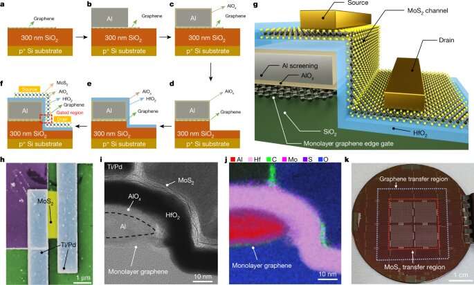
The 0.34 nm gate-length side-wall monolayer MoS2 transistor device structure and characterization. Credit: Nature (2022). DOI: 10.1038/s41586-021-04323-3
A team of researchers working at Tsinghua University in China has created a sub-1-nm gate in a MoS2 transistor. In their paper published in the journal Nature, the group outlines how they created the super tiny gate and explains why they believe it will be difficult for anyone to beat their record.
For most of the history of microcomputing, Moore's Law has held up—researchers and engineers have managed to double the speed and capability of computers regularly by reducing the size of their components. But more recently, it has grown increasingly difficult to make components smaller as scientists now run into physical limitations. In this new effort, the researchers believe they may have bumped up against the ultimate limit—they have built a gate that is just one atom in length.
At their most basic, transistors are a source and a drain, with a gate controlling the flow of electricity between them. It switches on and off depending on how much electricity is applied. The push to reduce the size of the components has led to the testing of materials such as carbon nanotubes, which are approximately 1nm, for use as gates. In this new effort, the researchers have unrolled the carbon nanotube and used its graphene edge as the gate—reducing its length to just 0.34 nm.
To make their gate, and a source and drain to go along with it, the researchers created a multiple-layer sandwich of materials. The bottom silicon layer serves as a base, which was covered by a layer of graphene, followed by a layer of aluminum oxide. Next, they etched the material to remove the top layers from half of their transistor, leaving a stairstep configuration to expose the edge of the graphene layer, allowing its use as a gate. They then covered both parts of the transistor with a layer of hafnium oxide to create a channel between the source and drain and through the gate. Then finally, they added two metal electrodes, one on the upper part of the step to serve as the source and one on the lower part of the step to serve as the drain.
Getting down to the atomic level I would guess.
Good luck to these folks.
Not to worry. Our companies are working on getting your nano-transistors ready to correct incorrect pronouns.
1,000 nanometers in a micron.
Mind-boggling scale.
Gonna be a bitch to probe that gate!
Saw some handmade Opamp chips,and waveguide size of human hairs, made under a microscope at a seti lab in the late 80s
Had computers the size of a grain of sand then..
And find your face in a crowd no matter where you go.
I think that TSMC is producing 5nm now in volume. But still, less than 1nm is impressive.

Awesome,
I have been involved in many projects for the military and commercial robotics, instrumentation, like nira
Retired, glad I am, but holding regiater tolerance in a 10 color print on a 8 foot film web web moving 2000 foot per minute was fun.. I understand you’re grief..smile
Ahh sitting in woods writing code for machinery in another country was fun..
Nasa was also cool..
Can I weep with you...waaaa..smile..
That’s why I did this..lol
You’d think I’d know better..lol..engineers are the craziest, in a good way,folks there are..
https://rumble.com/vwd2iv-requiem-for-ukraine-and-the-world.html
They represent the smallest members in the group.
Huge if true
Why publish in a non refereed journal? And a non tech journal? These usually show up in an IEEE or Physics journal
Now THAT is a small MOA.
Okay, but try to keep it down.
We wouldn't want people to talk....
/s
Lol, I’m probably bad company to boot, not trampled yet..smile..
Disclaimer: Opinions posted on Free Republic are those of the individual posters and do not necessarily represent the opinion of Free Republic or its management. All materials posted herein are protected by copyright law and the exemption for fair use of copyrighted works.